

Bio
Dr. Md. Azizar Rahman was born in Naogaon, Bangladesh. He obtained B.Sc. (Honours) in Physics and M.Sc. in Solid State Physics from the University of Rajshahi. He secured his M.Phil. degree in Magnetic Materials from the Bangladesh University of Engineering and Technology (BUET) and Ph.D. in Semiconducting Nanomaterials from the University of Technology Sydney, Australia. He joined BUET in 2011 as a lecturer and was promoted to Assistant Professor in 2014, Associate Professor in 2021, and Professor in 2025.
Education & Training
-
Ph.D. 2019
Semiconducting Nanomaterials
University of Technology Sydney, Australia
-
M.Phil. 2011
Solid State Physics
Bangladesh University of Engineering and Technology
-
M.Sc. 2008
Solid State Physics
University of Rajshahi
-
B.Sc. 2006
Physics
University of Rajshahi
Honors, Awards and Grants
-
2017Australia Research Training Program (RTP) Scholarship

The International Postgraduate Research Scholarship (IPRS) was replaced by the Research Training Program (RTP) Scholarship from 1 January 2017.
-
2015International Postgraduate Research Scholarship (IPRS)
This scholarship is funded by the Department of Education, the Australian Government for the international PhD student.
-
2015Australian Postgraduate Award (APA)
This scholarship is funded by the Australian Government for the living expense of international PhD student.
-
2010NSICT fellowship
This fellowship is funded by the Ministry of Science and Technology, Government of Bangladesh for a local research student.
-
2009Best presentation Award
Bangladesh Physical Society
Publications
Filter by type:
Sort by year:
A transparent self-powered ZnVO2/CdGa2O3 heterostructure for integrating UV photodetection and luminescence down-conversion
Journal Paper Journal of Material Chemistry C 14 (2026) 12144
Abstract
The coupling of light detection, emission, and transmission, along with self-powering in a single optoelectronic chip, is required for next-generation, energy-efficient devices, yet remains severely challenging. Here, Zn-doped VO2 (ZnVO2) nanowire networks are grown on Cd-doped Ga2O3 (CdGa2O3) thin films to fabricate a transparent self-powered ZnVO2/CdGa2O3 heterostructure, which simultaneously enables ultraviolet (UV) photodetection and luminescence down-conversion under a single excitation source. Individually, Cd doping in Ga2O3 destabilizes the characteristic self-trapped hole-associated UV emission and produces a broad green luminescence band resulting from Cd-induced defect states, while Zn-doping introduces oxygen vacancies, stimulating the green luminescence in ZnVO2 along with the characteristic UV and yellow emissions originating from distinct recombination channels within its correlated electronic configuration. The heterostructure fabricated from ZnVO2 nanowires and CdGa2O3 films exhibits semiconductor diode-like rectifying characteristics and functions as a self-powered ultraviolet photodetector with a high sensitivity of 251 mA W−1 and a fast response time of 85 ms. The built-in field at the heterostructure interface promotes effective charge-carrier segregation and recombination under zero bias, producing bright orange-red luminescence visible to the naked eye when the device functions as a self-powered UV photodetector. In particular, this integrated device maintains ∼75% transparency and provides a clear view through the device architecture. This photodetector heterostructure absorbs 4.96–3.26 eV high-energy broadband UV light and converts it into low-energy orange-red luminescence covering 2.21–1.51 eV, reflecting efficient luminescence down-conversion. The coupling of broadband UV detection, visible-light emission, optical transparency, and self-powered operation into the ZnVO2/CdGa2O3 heterostructure makes it suitable for integrated photonics, photovoltaic windows, flexible display technologies, and luminescence down-conversion electrodes for photovoltaics.
Modulating the visible emission and whispering gallery mode lasing through the self-induced defects in a Ga-doped ZnO tapered microcavity
Journal Paper Materials Advances (2026)
Abstract
Achieving low-order visible whispering gallery mode (WGM) lasing in monolithic semiconductor microcavities is typically hindered by poorly controlled defect emission and limited dispersion control. We address this by co-designing the gain spectrum and cavity geometry in single, tapered Ga-doped ZnO (GZO) hexagonal microrods grown by vapor-phase deposition. Ga incorporation forms Ga–native-acceptor complexes that red-shift and broaden the deep-level band, creating a tunable 500–600 nm gain window. Concurrently, the built-in diameter gradient (0.73–2.5 µm) deterministically selects WGM order along the same resonator, enabling continuous tuning of WGM order from N = 29 to N = 3–5. Plane-wave analysis and finite-element simulations accurately reproduce the measured path lengths, mode numbers, and linewidth evolution. By uniting defect-state engineering with geometry control in a single cavity, without the use of coupled resonators, plasmonics, or heterostructures, this approach enables the delivery of compact, spatially addressable, low-order visible microlasers for integrated photonics.
Interface-engineered ZnVO2 nanowire/CdO–Ga2O3 heterophase junctions for self-powered UV photodetection and defect-mediated visible luminescence
Journal Paper Materials Today Nano 35 (2026) 100875
Abstract
Traditional optoelectronic devices are limited in functionality and performance to discrete applications, and integrating various functionalities in a single device remains challenging. Here, self-assembled Zn-doped VO2 (ZnVO2) nanowire networks are interfaced with crystalline CdO-Ga2O3 heterophase film to fabricate a semitransparent self-powered ZnVO2/CdO-Ga2O3 isotype heterostructure, in which the junction-interface engineering enables the light transmission, detection, and emission functionalities simultaneously under a single excitation source. The CdO-Ga2O3 heterophase film exhibits a high absorption coefficient of 1.6 × 105 cm−1, which enables the charge-carrier generation and recombination. ZnVO2 nanowire networks facilitate a highly transparent (85%) low-resistance path for carrier collection, resulting in a high photocurrent generation. The heterostructure exhibits an optical transparency of 62%, enabling clear vision through its architecture. This semitransparent ZnVO2/CdO-Ga2O3 heterostructure exhibits rectifying behaviour and operates as a self-powered detector with a fast response time of 60 ms and a high detectivity of 6.2 × 10¹¹ Jones. Simultaneously, this integrated device shows an intense orange emission observed by the naked eye during its self-powered detection, and this orange emission is attributed to the interfacial oxygen vacancy exhibiting a slow decay time constant of 17.2 μs, as confirmed by transient photoluminescence measurements. Mott-Schottky and X-ray photoemission experiments show that the formation of a high valence-band offset of 2.1 eV and a built-in electric field of 5.1 × 10⁶ V/m at the junction interface effectively separates the photogenerated carriers for self-powered operation. This metal-oxide-based nanostructured heterojunction can serve as a versatile optoelectronic platform for integrated UV sensing with visible readout, anticounterfeiting, and integrated photonics.
Temperature-dependent broadening of spectral lineshapes and kinetics of luminescence centers in monoclinic gallium oxide nanowires
Journal Paper Journal of Alloys and Compounds 1010 (2025) 177609
Abstract
The broadening of spectral lineshapes and kinetics of luminescence centers in highly crystalline monoclinic gallium oxide (β-Ga2O3) nanowires have been investigated through temperature-dependent cathodoluminescence (CL), transient photoluminescence (PL), as well as hybrid density functional theory (DFT). The results indicate that the holes are trapped onto two distinct sites of oxygen, forming two self-trap holes (STHs), namely STHO1 and STHO3, which are stable and optically active luminescence centers in β-Ga2O3 nanowires, depending on temperature. The nanowires exhibit an ultraviolet luminescence (UVL) band at room temperature. The spectral lineshape of this UVL band shows an asymmetric broadening with decreasing temperature, which leads to the emergence of a new deep ultraviolet luminescence (DUVL) band below 220 K. These UVL and DUVL bands in β-Ga2O3 nanowires are attributed to STHO3 and STHO1 luminescence centers, which show similar thermal quenching behavior and possess short decay time constants of 7.11 and 5.25 ns, respectively. Hybrid DFT calculations and simulation of the UVL and DUVL bands using the Franck-Condon model reveal the vibronic coupling strength, zero phonon energies, and self-trapping energies of STHO1 and STHO3.
Defect engineering and carrier dynamics in gallium-doped zinc oxide nanowires for light-emitting applications
Journal Paper Journal of Materials Chemistry C 13 (2025) 5814
Abstract
Gallium (Ga) dopant-induced modulation of defects and recombination dynamics in wurtzite zinc oxide (ZnO) nanowires are investigated by cathodoluminescence (CL) and transient photoluminescence (PL) spectroscopy, complemented by density functional theory (DFT). The results reveal that high doping levels of Ga (4 atom%) in ZnO nanowires grown in an oxygen-rich environment lead to the formation of GaZn–VZn intraband states, which act as optically active luminescence centers. The emission lines of Ga-induced donor-bound excitons and acceptor-bound complexes confirm the formation of GaZn and GaZn–VZn defects in Ga-doped ZnO nanowires. The presence of these bound complexes significantly reduces the bandgap and broadens the near-band edge (NBE) emission of ZnO. The formation of GaZn–VZn defects significantly suppresses the characteristic VZn-related green luminescence (GL) and introduces a new recombination channel of orange luminescence (OL). Temperature-dependent CL and time-resolved PL analyses reveal that this OL band, attributed to the GaZn–VZn center laying at 0.62 eV over the valence band, exhibits a slow decay time constant of 5.4 ms. The simulation of the spectral line shape of this OL band using the Franck–Condon model reveals the thermodynamic transition level of 630 meV above the valence band and an electron–phonon coupling strength of 6.4 for this OL center. Ga-doped ZnO nanowire arrays are used to fabricate nanowire-based light-emitting diodes (LEDs), which show a low threshold voltage of 4.1 volts and intense orange electroluminescence. These Gadoped ZnO nanowires grown in an oxygen-rich environment can be used as efficient orange-coloured light emitters in photonic and optoelectronic devices.
Cadmium defect-induced modulation of hole self-trapping in monoclinic gallium oxide for optoelectronic applications
Journal Paper Journal of Material Chemistry C
Abstract
Self-trap holes (STHs) in β-Ga2O3 prohibit p-type conduction in this material, severely limiting its homojunction-based optoelectronic applications. Here, we report that the presence of cadmium (Cd) impurity in β-Ga2O3 (CdGa2O3) drastically quenches STHs and significantly increases p-type conductivity in this material, making it promising for optoelectronics. Photoluminescence experiments show that Cd-induced defects in β-Ga2O3 significantly suppress the characteristic ultraviolet luminescence, indicating the reduction of STHs. The CdGa2O3 film shows the distinct recombination channels of green and blue emissions attributed to CdGa and VGa defects, which exhibit slow decay time constants of 38.45 and 13.31 μs, respectively. Density functional calculations reveal that a few atom% of Cd in β-Ga2O3 induces an intermediate valence band state due to the formation of CdGa and VGa defects in the octahedral sites. The calculated energy levels of CdGa and VGa defects are 0.72 and 0.18 eV, respectively, which are significantly lower than the energy level of 0.99 eV for STHs, resulting in the destabilization of STHs and promoting p-type conductivity. The Mott–Schottky measurement confirms the p-type conductivity in the CdGa2O3 film with an acceptor concentration of 3.65 × 1017 cm−3. This p-type CdGa2O3 film is used for fabricating Ag/p-CdGa2O3 Schottky diodes, which operate as high-performance self-powered ultraviolet photodetectors possessing a high responsivity of 164 mA W−1 and a specific detectivity of 7.5 × 10¹¹ Jones. This p-type CdGa2O3 film could provide better flexibility in designing efficient homojunction-based optoelectronic devices.
Zinc Dopant-Induced Modulation of Electronic Structure and Defect Emissions in Monoclinic Gallium Oxide
Journal Paper The Journal of Physical Chemistry C 128 (2024) 4722
Abstract
Zinc (Zn) is a promising dopant for inducing visible emissions in monoclinic gallium oxide (β-Ga2O3), however, the recombination mechanism of these emissions is unclear. Here, the effect of Zn dopant on the valence-band electronic structure and luminescence properties of nanocrystalline β-Ga2O3 films is investigated through chemical and optical analyses as well as density functional theory (DFT) simulations. The comparison between the DFT results and the photoemission spectra of the valence band and core levels shows the accuracy and consistency of structure optimization. The undoped β-Ga2O3 film exhibits a broad emission band consisting of two emission bands: ultraviolet (UV) at 3.3 eV and blue luminescence (BL) at 2.9 eV, characteristic of pure β-Ga2O3. Incorporation of Zn into the β-Ga2O3 film significantly changes the luminescence spectral line shapes, resulting in an additional green luminescence (GL) band at 2.45 eV alongside the characteristic UV and BL emissions, which are found to be strongly dependent on excitation energy. Furthermore, the simulation of the spectral line shapes of these emission bands from the Zn-doped film within the framework of the configuration-coordinate model reveals the intraband states responsible for these luminescence bands and their electron-phonon coupling strengths. The simulation results show that the UV, BL, and GL emissions can be attributed to the self-trapped hole, VGa, and ZnGa acceptor states, and their energy levels are found to be 0.6, 1.1, and 1.5 eV above the valence band, respectively.
Simulation and interpretation of zinc and nitrogen dopants induced defect emissions in monoclinic gallium oxide
Journal Paper Materials Today Physics 46 (2024) 101503
Abstract
Zinc (Zn) and nitrogen (N) are potential acceptor dopants for inducing visible emissions and p-type conductivity in monoclinic gallium oxide (β-Ga2O3), however, the poor understanding of these dopants and their recombination process severely limited the optoelectronic applications. Here, we investigate the zinc (Zn) and nitrogen (N) dopants-induced intraband states and the broadening of defect emission bands due to vibronic coupling of highly transparent β-Ga2O3 films through chemical and optical analyses, as well as density functional theory. Incorporating Zn and N in β-Ga2O3 shifts the valence band edge towards the Fermi level and introduces band tail states above the valence band maximum. The emission band from pure β-Ga2O3 becomes significantly broad with the incorporation of Zn and N resulting in two additional emission bands: green luminescence (GL) and red luminescence (RL) along with the characteristic ultraviolet luminescence (UVL) and blue luminescence (BL) of pristine β-Ga2O3. Furthermore, the defect states responsible for these UVL, BL, GL, and RL emissions and their phonon coupling strengths are estimated by simulating the spectral line shape of these emission bands using the configuration coordinate model. The simulation results indicate that the Zn and N dopants-induced intraband states are responsible for the GL, and RL bands. These intraband states are acceptors, which provide p-type conductivity in β-Ga2O3 film
Investigation of the Influence of Pressure on the Physical Properties and Superconducting Transition Temperature of Chiral Noncentrosymmetric TaRh2B2 and NbRh2B2
Journal Paper ACS Omega 8 (2023) 21813−21822
Abstract
TaRh2B2 and NbRh2B2 compounds exhibit noncentrosymmetric superconductivity with a chiral structure. Density functional theory-based ab-initio calculations have been executed to analyze the structural properties, mechanical stability, ductility/ brittleness behaviors, Debye temperature, melting temperature, optical response to incident photon energy, electronic characteristics, and superconducting transition temperature of chiral TaRh2B2 and NbRh2B2 compounds under pressure up to 16 GPa. Both the chiral phases are mechanically stable and exhibit ductile nature under the studied pressure. The maximum value of the Pugh ratio (an indicator of ductile/brittle behaviors) is observed to be 2.55 (for NbRh2B2) and 2.52 (for TaRh2B2) at 16 GPa. The lowest value of the Pugh ratio is noticed at 0 GPa for both these chiral compounds. The analysis of reflectivity spectra suggests that both the chiral compounds can be used as efficient reflecting materials in the visible energy region. At 0 GPa, the calculated densities of states (DOSs) at the Fermi level are found to be 1.59 and 2.13 states eV-1 per formula unit for TaRh2B2 and NbRh2B2, respectively. The DOS values of both the chiral phases do not alter significantly with applied pressure. The shape of the DOS curve of both compounds remains almost invariant with applied pressure. The pressure-induced variation of Debye temperatures of both compounds is observed, which may cause the alternation of the superconducting transition temperature, Tc, with applied pressure. The probable changing of Tc with pressure has been analyzed from the McMillan equation.
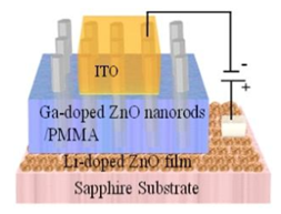
ZnO Nanorods on Li-Doped ZnO Thin Films for Efficient p-n Homojunction Light-Emitting Diodes
Journal Paper ACS Appl. Nano Mater. 6 (2023) 15757−15763
Abstract
Light-emitting diodes (LEDs) based on wide-bandgap ZnO have attracted widespread attention for use in solid-state lighting; however, their development has been hindered by the lack of a reliable, high-quality homojunction. In this work, an efficient p-n homojunction LED is fabricated based on the secondary growth of Ga-doped ZnO (GZO) nanorods onto a p-type Lidoped ZnO (LZO) thin film. Structural analyses reveal that both the GZO nanorods and LZO films possess a hexagonal structure with a c-axis orientation, and their crystalline quality is not affected by the incorporation of Ga or Li. The GZO nanorods with 4 atom % Ga and LZO films with 12 atom % Li show optimum optical and electrical properties. The homojunction fabricated from optimized GZO nanorods and LZO films exhibits the rectifying characteristics of a p-n junction LED with a low turn-on voltage of 3.2 V and a bright-yellow-orange electroluminescence (EL) band centered at 2.0 eV. Both the EL and electrical properties of the homojunction are found to be stable over a period of 2 months. The optimized LED based on the GZO nanorods is 16 times more efficient in EL than the equivalent device made from ZnO nanorods. The EL emission of the GZO/LZO homojunction can be explained by the formation of GaZn-VZn and LiZn deep-level defects induced by the incorporation of Ga and Li. These findings open opportunities to employ a doped ZnO homojunction as a highly efficient EL source in photonic devices.
Tuning the magnetic and magnetoelectric response in Bi1-xYxFe0.7Mn0.3O3 multiferroics
Abstract
Magnetoelectric (ME) coupling in multiferroic materials plays an important role in designing multifunctional devices because of their potential to tune polarization via a magnetic field or magnetism via an electric field. However, the single-phase ME materials have not been successfully explored in practical devices due to their low ME coupling coefficient. Here, we optimized the magnetic and magnetoelectric response of single-phase Bi1- xYxFe0.7Mn0.3O3 compounds by controlling the Y substitution and sintering temperature. Single-phase Bi1- xYxFe0.7Mn0.3O3 (where x varies from 0 to 0.20 in the step of 0.05) compounds were prepared by a standard solid-state reaction technique. The optimum sintering temperature and yttrium substitution were found to be 825 ◦C and x = 0.10, respectively, in which the sample shows the optimum microstructural, magnetic, and ME properties at room temperature. The optimized Bi0.9Y0.1Fe0.7Mn0.3O3 compound shows uniform growth of grains with less porosity, maximum remanent magnetization (~0.012 emu/g), and enhanced ME coupling coefficient (35 mV/Oe.cm.). The ME coupling coefficient obtained from the optimized sample is six times higher than that of the pristine sample. This work provides a potential route for improving the ME coupling coefficient in BiFeO3-based multiferroic materials for practical applications.
Physical and Superconducting Properties of Chiral Noncentrosymmetric TaRh2B2 and NbRh2B2: A Comprehensive DFT Study
Journal Paper ACS Applied Electronic Materials, 4 (2022) 1143
Abstract
TaRh2B2 and NbRh2B2 possess a chiral structure with noncentrosymmetric superconductivity. To explore their fascinating physics and physical properties, an ab-initio density functional theory (DFT) approach is used. The structural aspects, mechanical properties, electronic features, thermophysical and superconducting properties of TaRh2B2 and NbRh2B2 compounds are investigated and thoroughly discussed. This study provides a detailed valuable insight into the mechanical and optical properties of chiral noncentrosymmetric TaRh2B2 and NbRh2B2 compounds for the first time. The structural parameters are optimized using DFT and are in well accordance with experimental reports. This study reveals that both compounds are mechanically stable, ductile, and machinable. The estimated melting temperatures of TaRh2B2 and NbRh2B2 are ∼2302 and ∼2194 K, respectively. Various anisotropy indices reveal the anisotropic nature of these compounds. The analysis of optical functions suggests that both compounds might be suitable as prominent reflectors. The study of density of states (DOS) exhibits that the d orbital contribution is the most prominent near the Fermi level, EF. The evaluated total DOS values at EF are 1.60 and 1.79 states/eV/fu for TaRh2B2 and NbRh2B2, respectively. The estimated electron- phonon coupling constants using the inverted McMillan equation are ∼0.585 and ∼0.618 for TaRh2B2 and NbRh2B2, respectively, which agree well with the previous report.
Convertible Green Luminescence Determined by Surface Band Bending in ZnO
Journal Paper Journal of Physical Chemistry C, 126 (2022) 4082
Abstract
Green luminescence (GL) of ZnO is a typical defect emission and an important research topic for defect-controlling engineering. Two kinds of spectral characteristics, namely, Gaussian GL (GGL) and fine-structure GL (FSGL), are designated from a variety of spectra. It is found that GGL and FSGL can be reversibly converted through surface modification techniques where the location of the recombination center, the surface state, or the degree of band bending is modified. This convertible feature proves that the carrier recombination could be precisely controlled by surface modification. On the other hand, the effect of surface treatment on defects has achieved an unambiguous understanding, which is beneficial to effectively improve the performance of ZnO devices.
Multi-wavelength emission through self-induced defects in GaZnO microrods
Journal Paper Journal of Alloys and Compounds, 895 (2021) 162693
Abstract
Multi-wavelength emission in wide bandgap semiconductors is commonly achieved through ternary alloying or quantum size effects. However, multi-wavelength emission within a single microstructure is highly challenging using these approaches. Here, we demonstrate that the luminescence wavelength within individual GaZnO microrods can be tailored via defect engineering. Fast chemical vapor growth of oxygenrich ZnO microrods with Ga2O3 as an additive in the ZnO vapour leads to formation of a tapered morphology with graded distribution of Ga dopants, while the Ga incorporation does not significantly alter their crystal structure. With increasing Ga content from 1 to 6 at% from tip to base, the GaZnO microrods increase in diameter towards the substrate in accordance with the birth-and-spread mechanism. The local near-bandedge emission within single ZnO microrods, analyzed by nanoscale cathodoluminescence spectroscopy, exhibits a red shift of ~0.6 eV with increasing Ga content and exhibits signature characteristics of an excitonic emission. Density Functional Theory calculations reveal that the variation in the emission wavelength arises from bandgap narrowing due to the merging of the electronic states of Ga defect complexes with ZnO energy bands. The experimental and theoretical results demonstrate (i) the utility of using the self-regulation of defect compensation effects for band gap engineering and (ii) the possibility of multiwavelength light sources within individual microrods.
Electrical and optical properties in O-polar and Zn-polar ZnO films grown by pulsed laser deposition
Journal Paper Thin Solid Films 711 (2020) 138303
Abstract
O-polar and Zn-polar ZnO films were grown on c-sapphire by pulsed laser deposition. Positron annihilation spectroscopy study reveals that the VZn-related defects in the ZnO films with different polarities are different in structure and their thermal evolution is different. Hall effect measurement and luminescence spectroscopy reveal that the electrical and optical properties and their corresponding thermal evolution are strongly dependent on the polarity of the film. The luminescence spectra of the as-grown Zn-polar ZnO film is signified by a negligible green defect emission (at ~ 2.4 eV) and strong near band edge emission as compared with the O-polar film. The as-grown Zn-polar film exhibited a lower electron concentration (2 × 1018 cm−3) than that of the O-polar film (6 × 1018 cm−3); this difference is attributed to their different H concentrations. For the O-polar film, the electron concentration decreased with annealing temperature Tanneal, reaching a minimum at 700°C and then increased to 4 × 1018 cm−3 at Tanneal = 900 °C. In comparison, the electron concentration of the Zn-polar ZnO film monotonically decreased with Tanneal attaining a value of ~1 × 1017 cm−3 at Tanneal = 900 °C, 40 times smaller than that of the O-polar film. The cause for the differences in the optical and electrical properties for the O-polar and Zn-polar films is explained by the presence of different defects in these films.
Structural, optoelectronic characteristics and second harmonic generation of solution-processed CH3NH3PbI3-xClx thin film prepared by spray pyrolysis
Journal Paper Materials Science and Engineering: B 259 (2020) 114599
Abstract
Nanorod like crystalline CH3NH3PbI3-xClx thin film was prepared by spray pyrolysis at an ambient atmosphere. X-ray diffraction (XRD) and Raman studies reveal the tetragonal perovskite phase of spray deposited film. The optical band gap of CH3NH3PbI3-xClx is estimated to ~1.64 eV which is consistent with vacuum-based deposited perovskites. The CH3NH3PbI3-xClx film exhibits a high absorption coefficient of the order of 106 m−1. Photoluminescence (PL) study suggests that band-to-band radiative recombination occurs in CH3NH3PbI3-xClx film. Cathodoluminescence study confirms the emission of 1.67 eV at 80 K and 1.80 eV at 300 K. In this study, the second harmonic generation at photon energy 3.6 eV is reported for the first time at room temperature (RT). It is noted that the band edge peak position at 1.67 eV is being diffused and shifted to 1.80 eV at RT while the second harmonic peak position at 3.6 eV remains unchanged.
Surface polarity control in ZnO films deposited by pulse laser deposition
Journal Paper Applied Surface Science 483 (2019) 1129
Abstract
We demonstrate a simple and inexpensive method of surface polarity control of ZnO grown by pulsed laser deposition (PLD). The polarity control is achieved in a straightforward way by changing the thickness of MgO buffer layer. The Zn- and O-polar ZnO films possess very distinct growth rate, electron concentration and mobility as well as different defect structures. These different structural and electronic properties result in significant differences in surface reactivity and device performance. For example, Pd Schottky diodes fabricated onto the O-polar ZnO film exhibit lower barrier height and ideality factor compared with the equivalent Zn-polar devices, while methylammonium lead iodide perovskite films are readily formed on O-terminated and rapidly decompose on Zn-terminated surfaces. This can be attributed to higher photocatalytic activity of Zn-terminated surface, as well as higher surface coverage of adsorbed hydroxyl groups. Consequently, our results indicate that polarity engineering to obtain favorable O-terminated surface can result in improved performance of ZnOcontaining optoelectronic devices, while Zn-terminated surfaces could be of interest for photocatalytic and sensing applications.
Cluster in ZnO films grown by pulsed laser deposition
Journal Paper Scientific Reports 9 (2019) 3534
Abstract
Undoped and Ga-doped ZnO films were grown on c-sapphire using pulsed laser deposition (PLD) at the substrate temperature of 600oC. Positron annihilation spectroscopy study (PAS) shows that the dominant VZn-related defect in the as-grown undoped ZnO grown with relative low oxygen pressure P(O2) is a vacancy cluster (most likely a VZn-nVOcomplex with n = 2, 3) rather than the isolated VZn which has a lower formation energy. Annealing these samples at 900o C induces out-diffusion of Zn from the ZnO film into the sapphire creating the VZn at the film/sapphire interface, which favors the formation of vacancy cluster containing relatively more VZn. Increasing the P(O2) during growth also lead to the formation of the vacancy cluster with relatively more VZn. For Ga-doped ZnO films, the oxygen pressure during growth has significant influence on the electron concentration and the microstructure of the VZn-related defect. Green luminescence (GL) and yellow luminescence (YL) were identified in the cathodoluminescence study (CL) study, and both emission bands were quenched after hydrogen plasma treatment. The origin of the GL is discussed.
Surface polarity control in ZnO films deposited by pulsed laser deposition
Journal Paper Applied Surface Science 483(2019) 1129
Abstract
We demonstrate a simple and inexpensive method of surface polarity control of ZnO grown by pulsed laser deposition (PLD). The polarity control is achieved in a straightforward way by changing the thickness of MgO buffer layer. The Zn- and O-polar ZnO films possess very distinct growth rate, electron concentration and mobility as well as different defect structures. These different structural and electronic properties result in significant differences in surface reactivity and device performance. For example, Pd Schottky diodes fabricated onto the O-polar ZnO film exhibit lower barrier height and ideality factor compared with the equivalent Zn-polar devices, while methylammonium lead iodide perovskite films are readily formed on O-terminated and rapidly decompose on Zn-terminated surfaces. This can be attributed to higher photocatalytic activity of Zn-terminated surface, as well as higher surface coverage of adsorbed hydroxyl groups. Consequently, our results indicate that polarity engineering to obtain favorable O-terminated surface can result in improved performance of ZnO-containing optoelectronic devices, while Zn-terminated surfaces could be of interest for photocatalytic and sensing applications.
Solution-processed mixed halide CH3NH3PbI3−xClx thin films prepared by repeated dip coating
Journal Paper Journal of Materials Science 54 (2019) 11818
Abstract
The mixed halide CH3NH3PbI3−xClx crystalline thin film has been prepared by two-step solution-processed repeated dip-coating method at an ambient atmosphere. X-ray diffraction study reveals the presence of tetragonal and cubic phases in the deposited film. Raman study confirms the metal halide bond in the inorganic framework and organic CH3 stretching/bending of C–H bond in CH3NH3PbI3−xClx perovskite. Scanning electron microscopy shows that cuboid and polyhedral-like crystal grains of 100 nm to 2 μm may find applications in optoelectronics. The perovskite CH3NH3PbI3−xClx thin film shows high spectral absorption coefficient of the order of 106 m−1. In the optical band gap study, we found the coexistence of cubic and tetragonal perovskite phases. The energy band gap is dominated by cubic phase having Eg = 2.50 eV over the tetragonal phase with bandgap Eg = 1.67 eV. The room-temperature photoluminescence study confirms band edge, shallow and deep-level emissions. The temperature-dependent cathodoluminescence study shows red, green and ultraviolet emissions. The dominating green luminescence evolved for the cubic phase at 2.51 eV. The red and ultraviolet emissions are also found for mixed-phase CH3NH3PbI3−xClx thin film, suitable for preparation of light-emitting devices.
A facile method for bright, colour-tunable light-emitting diodes based on Ga-doped ZnO nanorods
Journal Paper Nanotechnology 29 (2018) 425707
Abstract
Bottom-up fabrication of nanowire-based devices is highly attractive for oxide photonic devices because of high light extraction efficiency; however, unsatisfactory electrical injection into ZnO and poor carrier transport properties of nanowires severely limit their practical applications. Here, we demonstrate that ZnO nanorods doped with Ga donors by in situ dopant incorporation during vapour-solid growth exhibit superior optoelectronic properties that exceed those currently synthesised by chemical vapour deposition, and accordingly can be electrically integrated into Si-based photonic devices. Significantly, the doping method was found to improve the nanorod quality by decreasing the concentration of point defects. Light-emitting diodes (LEDs) fabricated from the Ga-doped ZnO nanorod/p-Si heterojunction display bright and colour-tunable electroluminescence (EL). These nanorod LEDs possess a dramatically enhanced performance and an order of magnitude higher EL compared with equivalent devices fabricated with undoped nanorods. These results point to an effective route for large-scale fabrication of conductive, single-crystalline ZnO nanorods for photonic and optoelectronic applications.
Multi-Color excitonic emissions in chemical dip-coated organolead mixed-halide perovskite
Journal Paper ChemistrySelect 3 (2018) 6525
Abstract
Organolead mixed‐halide perovskites capable of emitting multiple colors not only allow the fabrication of compact devices but also improves the functionality of light emitting devices beyond conventional displays. Here we demonstrate a cost‐effective chemical dip‐coating technique to grow highly reproducible methylammonium‐lead‐halide perovskite film, which exhibits highly efficient multi‐color emissions of red, green and ultraviolet. The power‐ and temperature‐resolved cathodoluminescence analyses reveal that these emissions are attributed to localized excitions with thermal activation energies of 27, 29 and 57 meV. The non‐linear fitting of these emission band widths within the frame work of Boson model reveals that excitons are strongly coupled to the lattice with energy of 28 meV, which is consistent with the Raman measurement. This work presents an effective method for the deposition of high‐quality and large‐area perovskite film, which could be useful for high‐performance multi‐color display devices.
Charge state switching of Cu acceptors in ZnO nanorods
Journal Paper Applied Physics Letter 110 (2017)121907
Abstract
Undoped and Ga-doped ZnO nanorods both exhibit an intense green luminescence (GL) band centered at 2.4 eV. Unlike the defect-related GL in undoped nanorods, the GL band in Ga-doped nanorods displays a periodic fine structure separated by 72 meV, which consists of doublets with an energy spacing of 30 meV. The emergence of the structured GL is due to the Cu+ state being stabilized by the rise in the Fermi level above the 0/-(Cu2+/Cu+) charge transfer level as a result of Ga donor incorporation. From a combination of optical characterization and simulation using the Brownian oscillator model, the doublet fine structures are shown to originate from two hole transitions with the Cu+ state located at 390 meV above the valence band.
Efficient multi-coloured Li-doped ZnO thin films fabricated by spray Pyrolysis
Journal Paper Journal of Alloys and Compounds 691 (2017) 339
Abstract
Undoped and Li-doped ZnO films with bright visible luminescence have been fabricated by the spray pyrolysis technique at 400 C. The pyrolytic films exhibit multi-coloured emissions of yellow, green and blue, which can be tuned by varying the Li concentration. Simulation of the cathodoluminescence spectra from the Li-doped films using the Huang-Rhys model reveals the energies of the luminescence centres and their electron-phonon coupling strength. These centres are attributable to either VZn or LiZnacceptor states. This work presents a practical route to fabricate inexpensive multi-coloured light-emitting coatings on any substrate.
Effect of Co doping on structural, optical, electrical and thermal properties of nanostructured ZnO thin films
Journal Paper Journal of Semiconductor 36 (2015) 033004
Abstract
Nanocrystalline Zn1-xCoxO (where x varies from 0 to 0.04 in steps of 0.01) thin films were deposited onto glass substrate by the spray pyrolysis technique at a substrate temperature of 350 °C. The X-ray diffraction patterns confirm the formation of hexagonal wurtzite structure. The crystal grain size of these films was found to be in the range of 11& 36 nm. The scanning electron micrographs show a highly crystalline nanostructure with different morphologies including rope-like morphology for undoped ZnO and nanowalls and semispherical morphology for Co-doped ZnO. The transmittance increases with increasing Co doping. The optical absorption edge is observed in the transmittance spectra from 530 to 692 nm, which is due to the Co2+ absorption bands corresponding to intraionic d-d* shifts. The direct and indirect optical band gap energies decrease from 3.05 to 2.75 eV and 3.18 to 3.00 eV, respectively for 4 mol% Co doping. The electrical conductivity increases with increasing both the Co doping and temperature, indicating the semiconducting nature of these films. The temperature dependence thermal electromotive force measurement indicates that both undoped and Co-doped ZnO thin films show p-type semiconducting behavior near room temperature. This behavior dies out beyond 313 K and they become n-type semiconductors.
Relaxation mechanism of (x) Mn0.45Ni0.05Zn0.50Fe2O4+(1-x) BaZr0.52Ti0.48O3 multiferroic composites
Journal Paper Physica Scripta 89 (2014) 115811
Abstract
Polycrystalline (x) Mn0.45Ni0.05Zn0.50Fe2O4+(1-x) BaZr0.52Ti0.48O3 (with 0.2 >x>0.8) multiferroic materials were prepared by the standard solid state reaction technique and samples prepared from these composites were sintered at 1200oC. The impedance, electrical modulus, ac conductivity and dielectric permittivity were investigated over a wide range of frequencies (20 Hz–1 MHz) and at various temperatures (room temperature to 600o C) to understand the relaxation phenomenon in these materials. X-ray diffraction patterns confirm the presence of a simple cubic spinel structure for the ferromagnetic phase and tetragonal peroveskite for the ferroelectric phase. Frequency-independent conductivity was observed in the low-frequency region, which shifts to a higher frequency and dominates over a wide range of frequency (up to 1 MHZ) at higher temperature (600o C). The transition temperature (~675oC) of these composites is higher than that of ferrite and ferroelectric phases. The frequency response electric modulus graphs for some composites show two maxima in the relaxation process. The first relaxation process appears at lower temperature and higher frequency with a lower value of activation energy for the composites containing more than 20% ferrimagnetic phase. This relaxation process is due to the first ionization energy of oxygen vacancies. The second relaxation process appears at all temperatures and at lower frequency, which shifts to higher frequency with increasing temperature, possessing a comparatively higher value of activation energy. This relaxation process is attributed to the Maxwell-Wagner-Sillars relaxation phenomenon. The frequency-dependent impedance and modulus plots exhibit a non-coincidence of relaxation peaks, indicating the deviation from the Debye-type relaxation process.
Structural and electrical properties of (x) Mn0.45Ni0.05Zn0.50Fe2O4+ (1-x) BaZr0.52Ti0.48O3 multiferroic materials
Journal Paper Materials Research Express 01 (2014) 026113
Abstract
Multiferroic (x)Mn0.45Ni0.05Zn0.50Fe2O4+(1-x)BaZr0.52Ti0.48O3materials (where x varies from 0.0 to 0.8 in steps of 0.20) were prepared by the standard solid-state reaction method. X-ray diffraction patterns verify the development of tetragonal perovskite structure for ferroelectric and cubic spinel structure for ferrite phase. The frequency and temperature-dependent electrical parameters have been investigated to understand the conduction mechanism in these multiferroic materials. The grain effect contributes to the conduction mechanism for the sample containing 0–60% ferrite and both the grain and grain boundary effect contribute to the conduction mechanism for the composite containing 80% ferrite at high temperature. The ac conductivity increases with increasing frequency for the sample x=0. This is due to the small polaron hopping. For the sample containing 20% ferrite, the frequency-independent dc conductivity is observed at low temperature and dominates over a wide frequency range at the high-temperature region for the sample containing a higher percentage of ferrite. The frequency-independent dc conductivity is shifted to the frequency-dependent ac conductivity, indicating the beginning of the conductivity relaxation phenomenon. This is attributed to the translation of long-range polaron hopping to the small range charge carriers. The temperature dependence conductivity indicates that the impurities present in these multiferroic materials are almost minimized and polaron hopping type of conduction mechanism is valid.
Effect of Cu2+ substitution on structural, magnetic and transport properties of Fe2.5Zn0.5-xCuxO4
Abstract
Polycrystalline Fe2.5Zn0.5−xCuxO4 ferrites (where y varies from 0 to 0.45 in steps of 0.05) were prepared by the standard solid state reaction technique. The X-ray diffraction patterns consist of major cubic spinel Fe2.5Zn0.5−xCuxO4 phase with minor impurity phases (Fe2O3 and CuO). The lattice constant decreases slightly with increasing Cu content. The bulk density and average grain size increases with Cu content up to x=0.30 due to the lattice diffusion. The initial permeability and relative quality factor increases with increasing Cu content up to x=0.30. It is attributed to the migration of Fe3+ in the octahedral sublattice and a decrease beyond this content is due to the spin canting effect. The dielectric constant and loss tangent decrease with increasing frequency of the applied alternating electric field because of dielectric polarization, which is similar to the conduction phenomenon. The ac conductivity increases with increasing frequency for the samples x≤0.15 due to the small polaron hopping conduction. The frequency-independent conductivity is found below a certain frequency for the samples x≥0.20 and dominated over a wide frequency range (up to 0.5 MHz) for the sample containing x=0.30 due to band conduction.
Effect of annealing temperature on structural, electrical and optical properties of spray pyrolytic nanocrystalline CdO thin films
Abstract
Nanocrystalline CdO thin films were prepared onto a glass substrate at substrate temperature of 300 °C by a spray pyrolysis technique. Grown films were annealed at 250, 350, 450 and 550 °C for 2.5 h and studied by the X-ray diffraction, Hall voltage measurement, UV-spectroscopy, and scanning electron microscope. The X-ray diffraction study confirms the cubic structure of as-deposited and annealed films. The grain size increases whereas the dislocation density decreases with increasing annealing temperature. The Hall measurement confirms that CdO is an n-type semiconductor. The carrier density and mobility increase with increasing annealing temperature up to 450 °C. The temperature dependent dc resistivity of as-deposited film shows metallic behavior from room temperature to 370 K after which it is semiconducting in nature. The metallic behavior completely washed out by annealing the samples at different temperatures. Optical transmittance and band gap energy of the films are found to decrease with increasing annealing temperature and the highest transmittance is found in near infrared region. The refractive index and optical conductivity of the CdO thin films enhanced by annealing. Scanning electron microscopy confirms formation of nano-structured CdO thin films with clear grain boundary.
Relaxation and conduction mechanisms of high Tc lead-free Ba(Zr,Ti)O3 positive temperature coefficient of resistivity ceramic using impedance spectroscopy
Abstract
High Tc lead–free Ba (Zr0.52Ti0.48)O3 positive temperature coefficient of resistivity (PTCR) ceramic was produced by the standard solid state reaction technique. X–ray diffraction pattern confirms the formation of the tetragonal perovskite structure of the ferroelectric sample. The conduction and relaxation mechanisms of the piezoelectric ceramic have been studied on the basis of activation energy. The relaxation mechanism is investigated for this sample based on the peaks of the imaginary part of electrical impedance and modulus spectra. The Cole-Cole plots indicate that the grain effect is influenced by the increase of temperature up to 200 °C and disappeared beyond this temperature. The temperature versus electrical resistivity plots show that a phase transition occurs at the Curie temperature, Tc =150 °C. The ceramic exhibits a PTCR jump of almost two orders of magnitude starting at 150 °C and ending at 275 °C with a high temperature coefficient of resistivity of ~25 % per °C. The electrical resistivity measurements also reveal that the sample shows semiconducting behavior beyond 275 °C with the value of negative temperature coefficient of resistivity of ~ 0.6% per °C.
Electrical transport properties of Mn-Ni-Zn Ferrite using complex impedance spectroscopy
Journal Paper Physica Scripta 89 (2014) 025803
Abstract
Polycrystalline Mn0.45Ni0.05Zn0.50Fe2O4 was prepared by a standard solid state reaction technique. We report the electrical properties of this ferrite using ac impedance spectroscopy as a function of frequency (20 Hz–10 MHz) at different temperatures (50–350 °C). X-ray diffraction patterns reveal the formation of cubic spinel structure. Complex impedance analysis has been used to separate the grain and grain boundary resistance of this ferrite. The variation of grain and grain boundary conductivities with temperature confirms semiconducting behavior. The dielectric permittivity shows dielectric dispersion at a lower frequency and reveals that it has almost the same value on the high-frequency side. The non-coincidence of peaks corresponding to modulus and impedance indicates deviation from Debye-type relaxation. A similar value of activation energy is obtained from impedance and modulus spectra, indicating that charge carriers overcome the same energy barrier during relaxation. Electron hopping is responsible for ac conduction in this ferrite. The electron hopping shifts toward higher frequency with increasing temperature, below which the conductivity is frequency independent. The frequency-independent ac conductivity has been observed at and above 300 °C in the frequency range 20 Hz–1 MHz. This frequency-independent ac conductivity is due to the long-range movement of the mobile charge carriers.
Structural, magnetic and transport properties of magnetoelectric composites
Abstract
Magnetoelectric composites of nominal chemical compositions (y)Mn0.45Ni0.05Zn0.50Fe2O4+(1−y)BaZr0.52Ti0.48O3 (where y varies from 0 to 1.0 in steps of 0.20) were prepared by the standard solid state reaction technique. The samples were sintered at various temperatures. X-ray diffraction patterns confirm the presence of the constituent phases. The initial permeability increases with increasing ferrite content and also with increasing sintering temperature. However, there is a slight decrease in initial permeability value for samples sintered above 1573 K. The dielectric dispersion is observed at lower frequencies (<103 Hz) due to interfacial polarization. The dielectric constant is almost independent at high frequencies (>104 Hz) for a particular composition because of the inability of electric dipoles to follow the fast variation of the alternating applied electric field. The ac electrical conductivity increases with increasing frequency, suggesting that the conduction is due to small polaron hopping. The increase in dielectric constant and dielectric loss corresponds to the increase in ac electric conductivity with increasing sintering temperature up to 1573 K. The magnetoelectric voltage coefficient of the composites decreases with increasing ferrite content and dc magnetic field.
Effect of Al-doping on optical and electrical properties of spray pyrolytic nano-crystalline CdO thin films
Journal Paper Current Applied Physics 10 (2010) 790
Abstract
CdO and Al-doped CdO nano-crystalline thin films have been prepared on glass at 300 °C substrate temperature by spray pyrolysis. The films are highly crystalline with grain size (18–32 nm) and found to be cubic structure with lattice constant averaged to 0.46877 nm. Al-doping increased the optical transmission of the film substantially. Direct band gap energy of CdO is 2.49 eV which decreased with increasing Al-doping. The refractive index and dielectric constant varies with photon energy and concentration of Al as well. The conductivity of un-doped CdO film shows metallic behavior at lower temperature region. This behavior dies out completely with doping of Al and exhibits semiconducting behavior for whole measured temperature range. Un-doped and Al-doped CdO is an n-type semiconductor having carrier concentration is of the order of ∼1021 cm−3, confirmed by Hall voltage and thermo-power measurements.
Structural transition and Multi-Color Emissions in Chemical Dip-Coated Organolead MixedHalide Perovskite
Abstract
Activating Cu luminescence centres in ZnO nanorods by Ga doping
Abstract
Undoped and Ga-doped ZnO (GZO) nanorods both exhibit an intense green luminescence (GL) band centered at ~ 2.4 eV. Unlike the defect-related GL in ZnO nanorods, the GL band in GZO nanorods displays a periodic doublet structure separated by 72 meV. It is shown in this paper that the emergence of the structured GL is due to the Cu + state being stabilized by the rise in the Fermi level above the 0/-(Cu 2+ /Cu +) charge transfer level as a result of Ga donor incorporation.
Structured green emission band and electron-phonon coupling in Ga-doped ZnO nanowires
Abstract
Ga doping of ZnO can tailor the optoelectronic properties of this material and open up new possible applications such as tunable plasmonic devices1. In this work, ZnO and Ga-doped ZnO (GZO) nanowires have been synthesized using the vapour phase transport method. The longitudinal optical (LO) phonon structures are well resolved in the green luminescence (GL) band of GZO nanowires but absent in the ZnO GL, indicating enhanced electron-phonon coupling. This phonon coupling is investigated by simulating the GL spectra within the framework of the multimode Brownian oscillator model.
Response of Dielectric Behaviour in Piezoelectric and Magnetostrictive Composites
Conference Paper IEEE Xplore digital Library (2012) 644-647
Abstract
The magnetoelectric composites consisting of ferrite and ferroelectric phases viz.(y)Mn 0.45 Ni 0.05 Zn 0.50Fe 2 O 4+ (1-y)BaZr 0.52 Ti 0.48 O 3 in which y varies from 0.20-0.80 mol% were prepared by standard solid state reaction method. X-ray analysis of these composites confirms the presence of both the phases, i.e. ferroelectric and ferrite in the composites. Detailed studies of dielectric constant, loss tangent, and ac conductivity, as a function of frequency (20 Hz - 10 MHz) were studied. The dielectric constant decreases steeply at lower frequencies and remains constant at higher frequencies, indicating dielectric dispersion. This may be attributed to polarization due to changes in the valence states of cations and space charge polarization. Results of ac conductivity show that conduction occurs by hopping of charge carriers. The static magnetoelectric voltage coefficient was measured as a function of applied dc magnetic field. It decreases with increasing dc magnetic field. These composites may be useful as transducer, magnetic sensors, filter, etc.
Structural, Optical and Electrical Properties of CdO Thin Films Obtained by Spray Pyrolysis method
Abstract
Thin films of CdO sample were deposited on a glass substrate by spray pyrolysis method at 300 ˚C substrate temperature. The crystal structure of the CdO thin films is identified as cubic with lattice constant 4.68 Å from x-ray diffraction analysis. SEM micrograph shows that the surface of CdO is smooth with some precipitations. The absorption coefficient slowly increases with the increasing of photon energy in the lower energy region and then increases rapidly near the transition edge at 2.49eV. The direct and indirect bandgap energies is determined and found to be 2.49 eV and 2.17 eV respectively. The refractive index gradually increases with photon energy and reaches a maximum value near 1.5 eV and then gradually decreases. The real part of the dielectric constant shows the same pattern as the refractive index. The imaginary part of the dielectric constant remains almost constant in the lower energy region but increases rapidly at the transition edge. The resistivity CdO film increases monotonically with an increase in temperature up to 360 K and then decreases very slowly with temperature. These types of transparent conducting thin films are used in transparent electrodes in photovoltaic and display device, solar cells and sensors.
Structural, Dielectric and Electrical Properties of ferroelectric
(y)Mn0.45Ni0.05Zn0.50Fe2O4+(1-y)BaZr0.52Ti0.48O3 composites
Abstract
The magnetoelectric composites consisting of ferrite and ferroelectric phases viz. (y)Mn0.45Ni0.05Zn0.50Fe2O4+(1-y)BaZr0.52Ti0.48O3 in which y varies as 0.20, 0.40, 0.60 and 0.80 mol% were prepared by standard solid-state reaction method. X-ray diffraction patterns confirm the presence of the constituent phases, i.e. ferroelectric and ferrite phase in the composites. The electrical properties such as ac resistivity and conductivity were measured as a function of frequency (20 -120 MHz) of constituent phases. Results of ac conductivity show that conduction occurs by hopping of charge carriers. The variation of dielectric constant and loss tangent in the frequency range 20 Hz to 120MHz was also studied. The dielectric constant decreases steeply at lower frequencies and remains constant at higher frequencies, indicating dielectric dispersion. This may be attributed to polarization due to changes in the valence states of cations and space charge polarization. These composites may be useful as a transducer, magnetic sensors and filter.
Effect of composition on magnetic and dielectric properties of two-phase particulate magnetoelectric composite
Abstract
Two-phase particulate magnetoelectric (ME) composites with compositions (y)Mn0.45Ni0.05Zn0.50Fe2O4+(1-y)BaZr0.52Ti0.48O3 ( where y = 0.00, 0.20, 0.40, 0.60, 0.80 and 1.0) were prepared by standard solid-state reaction technique. X-ray diffraction patterns confirm the presence of the constituent phases, i.e. ferroelectric and ferrite phase in the composites. The electrical properties such as ac resistivity and conductivity were measured as a function of the frequency of constituent phases. It is observed that the conduction in the present composites is due to small polarons. The variation of dielectric constant and loss tangent (tan δ) in the frequency range 20 Hz to 120MHz was also studied. It shows dispersion in the lower frequency range. The complex permeability, loss factor and relative quality factor of all composites were studied in the frequency range from 100 Hz to 120MHz. As the ferrite content increases from 0 to 100%, at frequency 1 MHz the real part of the permeability increases from 11.30 to 25.62 and the imaginary part slightly increases from 1.30 to 1.57. The magnetic loss of the ferrite phase is high and the composites are very low. Quality factor decreases with increases ferrite content at a higher frequency above 10MHz for all composites. The static magnetoelectric (ME) voltage coefficient was measured as a function of the applied dc magnetic field. It decreases with increasing dc magnetic field. The ME conversion factor of 51.50 mV/cm.Oe was observed for the composite with 20%Mn0.45Ni0.05Zn0.50Fe2O4 +80%BaZr0.52Ti0.48O3. These composites may be useful as a transducer, magnetic sensors, filter, etc.
Preparation and characterization of Al doped CdO thin films prepared by spray pyrolysis method
Abstract
CdO and Al-doped CdO thin films have been prepared by spray pyrolysis method and studied their structural, surface, optical and electronic transport properties. The crystal structure of CdO and Al-doped CdO was found be cubic with lattice parameter a=4.68 Å. The surface of the film was studied by SEM which shows that the surface is homogeneous and quite smooth for higher doping concentration of Al. Direct bandgap energy of CdO determined from transmittance and reflectance spectra found to lie within 2.09-2.49 eV depending on Al concentrations. The refractive index and dielectric constant found to vary with photon energy and concentration of Al as well. The temperature-dependent resistivity of CdO shows metallic behavior at lower temperature region. The behavior dies out with doping of Al and exhibits semiconducting behaviour for whole temperature range completely. CdO and Al-doped CdO is an n-type semiconductor by Hall voltage and thermo-power measurements.
Abstract
In recent years, there has been resurgent interest in ZnO due to its efficient UV emission and potential application in opto-electronic devices. The problem of self-compensating defects, especially those related to acceptor-like dopants, remains a major challenge to date. In this chapter, we provide an overview of the fundamental properties of point defects and dopants as well as their complexes in bulk crystals and nanostructures. Nominally undoped ZnO is typically n-type, which has been widely ascribed to O vacancies or Zn interstitials; however, these defect assignments are controversial as O vacancies are deep donors while Zn interstitials are highly mobile at room temperature and considered to be unstable. Accordingly, H and group III impurities have also been suggested to be responsible for the observed n-type conductivity. Although there are still many unanswered questions concerning defect-related luminescence bands in ZnO, great progress has been made in recent years to identify and characterize them using spatially resolved luminescence spectroscopies and first-principles calculations. The ubiquitous green emission has several possible origins, including O and Zn vacancies as well as Cu impurities. The properties of group I (Li, Na, and Cu), group III (Ga, Al, and In), and group V (N, P, and Sb) impurities as well as their complexes with native point defects and H are discussed, along with a concluding outlook for future research into the optical properties of ZnO.
Recent Posts
Research Summary
His research is focused on semiconductor nanomaterials, quantum dots, defects in semiconductors, optoelectronics, and photonics.
Interests
- Defects in semiconductor materials
- Semiconducting nanomaterials
- Quantum dots
- Optoelectronics
- Photonics
Laboratory Personel
Synthesis methods: Spray pyrolysis, Hydrothermal, Sol-gel, Spin coating, Vapor phase transport
Characterization Techniques: Steady-state photoluminescence, Time-resolved photoluminescence, UV spectroscopy, Current-voltage characteristics, Photodetecting properties, Electrochemical work statation.
Fabrication facilities: p-n junctions, Light emitting diodes, Solar cells, Photodiodes,
Research Projects
-

Lead-free inorganic perovskites are leading in the race to commercialize solar cells and other photovoltaic devices. This study shows that metal (Cr/Mn)-doped CsSnCl3 perovskite exhibits high optical absorption, high photoconductivity, and high dielectric constant not only in the visible range but also in the ultraviolet range. Using density functional theory (DFT), we investigated the structural, electronic, optical and mechanical properties of pure CsSnCl3, Cr and Mn-doped CsSnCl3 samples. Investigation of the optical features shows that the absorption edges of both Cr- and Mn-doped CsSnCl3 are strongly shifted towards lower photon energy range (redshifted) compared to the pure samples. Especially high intensity absorption peaks are found in the visible energy range for both doped samples. Investigation of mechanical parameters shows that both Cr- and Mn-doped CsSnCl3 samples are mechanically stable and highly ductile compared to that of pure CsSnCl3 samples. Investigation of the electronic properties shows that the generation of intermediate states facilitates the valence-to-conduction band transition of excited photoelectrons for both the Cr- and Mn-doped CsSnCl3 samples. Combined analyzes suggest that Mn-doped CsSnCl3 is more suitable than the available inorganic metal halide perovskites for high-efficiency solar cell and other optoelectronic device applications.
-
Project starting date: 19-09-2022
Project Ending date: 18-09-2024
Principal investigator: Dr. Md. Azizar Rahman
-
Project starting date: August 2021
Project Ending date: Runing
Principal investigator: Dr. A. K. M. Akther Hossain
Co-investigator: Dr. Md. Azizar Rahman
-
Project starting date: July 2022
Project ending date: June 2023
Principal Investigator: Dr. Md. Azizar Rahman
Associate Investigator: Dr. A. K. M. Akther Hossain